

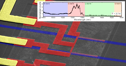
Keywords
Abstract
The work describes the use of a superconducting NbN detector for spectroscopy of an optical SiNx waveguide at cryogenic temperatures at single-photon power of the incident radiation in the S-, C-, and L-bands. The technological process of creating the superconducting detector on the planarized surface of a protective SiO2 layer over the SiNx optical waveguide is described. The transparency window of SiNx around 1550 nm was demonstrated as an increase in the number of optical counts of the detector.
Introduction
The most common platform for implementing compact optical circuits is based on Si\(^{\,}_3\)N\(^{\,}_4\) optical waveguides surrounded by SiO\(^{\,}_2\).[1] Optical spectroscopy in the \(L\)- and \(C\)-band wavelengths makes it possible to determine the characteristics of fabricated waveguides and the limits of their applicability.[2] One of the obstacles to performing single-photon spectroscopy of an optical waveguide is the optical fiber-photonic chip interface, which accounts for the greatest optical losses.[3] This work describes the technological process for fabricating SiN\(^{\,}_x\) waveguides surrounded by SiO\(^{\,}_2\) with integrated NbN superconducting single-photon detectors (SSPD) and with fabricated grooves (seating positions) for aligning the centers of the waveguide and the optical fiber. The superconducting detector was used for single-photon spectroscopy of the optical waveguide in the wavelength range from 1480 nm to 1640 nm at a temperature of 2.7 K.
Single-photon spectroscopy
Optical waveguides were formed on a silicon Si substrate with a 4 \(\mu\)m-thick thermally grown silicon dioxide SiO\(^{\,}_2\) buffer layer. A 400-nm-thick SiN\(^{\,}_x\) layer was deposited by inductively coupled plasma chemical vapor deposition (ICP-CVD) and patterned into waveguides with a width of 1.6 \(\mu\)m using optical lithography.[4] A scanning electron microscope (SEM) image of the fabricated waveguides is shown in blue in Figure 1a. The waveguides were subsequently coated with a SiO\(^{\,}_2\) cladding layer deposited by plasma-enhanced chemical vapor deposition (PECVD), which was then planarized to a thickness of 140 nm above the waveguide surface.[5]
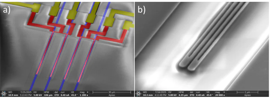
The superconducting detectors were fabricated from a 9-nm-thick NbN film deposited by reactive magnetron sputtering, with the meander structure defined by electron-beam lithography. The superconducting strips have a width of 120 nm and a total length of 600 \(\mu\)m, arranged in a W-shaped configuration, as shown in red in Figure 1a and Figure 1b. Contact pads were formed by a lift-off process using 200-nm-thick aluminum, also indicated in yellow in Figure 1a. As the final fabrication step, 62.5-\(\mu\)m-deep grooves were etched by the Bosch process to enable edge-coupling of light into the waveguides.
The fabricated chip, with optical fibers attached, was mounted in a closed-cycle cryostat and cooled to 2.7 K. Optical characterization was performed according to the setup shown in Figure 2a, with the chip placed in a custom-designed holder, as illustrated in Figure 2c.
The waveguide-integrated detector was biased with a direct current to a value of 0.9 of the critical current, which corresponds to a Dark Count Rate (DCR) \(\simeq 100\) Hz. The optical count rate (CPR) was on the order of \(10^6\) Hz, at which the system detection efficiency was approximately 2% at a wavelength of 1550 nm.
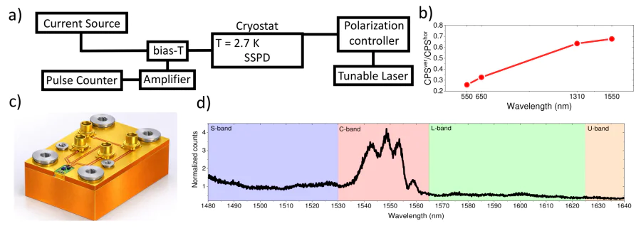
The polarization sensitivity of the fabricated SSPD was evaluated. Figure 2b presents the measured dependence of the photon-count ratio for vertical and horizontal polarizations.We defi ne horizontal polarization as coinciding with the plane of the optical waveguide width of 1.6 \(\mu\)m, and vertical polarization as coinciding with the plane of the optical waveguide height of 0.4 \(\mu\)m. The results clearly demonstrate that the polarization sensitivity decreases with increasing wavelength. This is attributed to the waveguide cross-section, in which the width is much greater than the height.
The laser wavelength was continuously swept from 1480 nm to 1640 nm at a rate of 1 nm\(\cdot\)s\(^{-1}\) to obtain the detector count rate as a function of wavelength averaged over 10 measurements, as shown in Figure 2d. The obtained dependence is normalized to the average optical count rate to demonstrate a significant change in the optical count rate with wavelength.The relative standard deviation for each measured wavelength value did not exceed 5% over 10 performed measurements. The polarization of the radiation was maintained vertical throughout the measurement using a polarization controller.
The wavelength dependence of the photon counts presented in Figure 2d exhibits distinct peaks at wavelengths of 1543 nm, 1549 nm, and 1553 nm. We compare our result with those reported by other research groups and find a good agreement in the overall lineshape of the obtained dependence.[6, 7] We attribute the shape of the dependence of the optical counts on the radiation wavelength to N–H absorption overtones, following the authors of the work who studied the spectral properties of the SiN\(_x\) film.[8] For more accurate conclusions, additional measurements of spectral characteristics are required, for example, using ring resonators.
Conclusion
This work reports on a superconducting NbN detector employed for single-photon spectroscopy of a SiN\(^{\,}_x\) optical waveguide, with the detector integrated onto the waveguide. The averaged photon-count rate as a function of wavelength was measured in the 1480–1640 nm range. We observe an increase in the photon count rate in the region of 1550 nm, which is consistent with observations from other independent groups performed at room temperature and at non-single-photon optical probing powers. It is suggested that the present results may be relevant for practical applications of SiN\(^{\,}_x\) optical waveguides under cryogenic conditions.
Acknowledgements
The study was supported by project No. 125020501540-9 of the Ministry of Education and Science of the Russian Federation. Fabrication and technology characterization were carried out at large scale facility complex for heterogeneous integration technologies and silicon+carbon nanotechnologies.
Contact information
Corresponding author: Mihail Dryazgov,
orcid.org/0000-0002-6280-4667,
e-mail dryazgovm@gmail.com
*
Proceedings of the II International Scientific Conference "Advanced functional materials for digital and quantum electronics' 26", September 14-18, 2026, Dolgoprudny, Russia
Funders
References


![Coupling strategies for silicon photonics integrated chips [Invited]](https://jmsn.colab.ws/storage/images/resized/bypZPcr6C4twKiQVCUCGc0GF4cH6aUWmpClD3hsH_small_thumb.webp)