

Keywords
Abstract
The apparent height h of a monatomic step on the upper surface of thin Pb(111) films, as measured by scanning tunneling microscopy in constant-current mode, is found to oscillate with bias voltage U. The oscillation period matches that of the local differential conductance dI/dU and the tip displacement rate dz/dU as the bias voltage is swept. This correlation indicates that the observed height variations originate from coherent resonant tunneling through quantum-well states in thin Pb(111) films. We argue that the extrema of the apparent step height occur at bias voltages where the differential tunneling conductances of Pb(111) terraces of different thicknesses are equal.
Introduction
Quantum confinement in low-dimensional systems gives rise to discrete energy levels, which often control the electronic properties of nanostructured solids [1, 2]. In thin metallic films, conduction electrons behave as quasi-free particles parallel to the surface, while their motion across the film is confined. This situation is analogous to the particle-in-a-box problem, yielding stationary solutions of the Schrödinger equation in the form of standing waves with an integer number of half-wavelengths within the film and evanescent tails in the barrier regions.[3] In scanning tunneling microscopy and spectroscopy linebreak (STM/STS), quantum-well states in systems with double potential barriers manifest themselves via coherent resonant tunneling, giving rise to a series of nearly equally spaced kinks in the current--voltage (\(I-U\)) characteristics and peaks in the voltage dependence of the differential conductance \(dI/dU\). [4-11] If tunneling through the barriers occurs incoherently, with phase-breaking effects (so-called sequential tunneling), these peaks in the \(dI/dU-U\) dependences become suppressed.[12]
Lead films and islands serve as a convenient platform for investigating various electronic and quantum-size effects by STM/STS [4-11], as well as by transport measurements [13, 14]. These systems have also been used to study the properties of superconducting nanostructures and two-dimensional superconductors [15-17], hybrid structures based on superconductors [18-22]. Importantly, the quantum-interference patterns are highly sensitive to variations in film thickness and to the structural quality of the interfaces. This sensitivity enables the spatial visualization of monatomic steps at the upper and lower film boundaries [4, 8, 9], embedded inclusions [9], terraces with non-quantized height variations [10], and even subsurface dislocation loops [11].
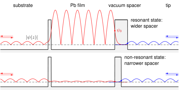
This paper examines how the local electronic properties of thin Pb(111) films, controlled by a quantum-size effect, influence STM topography measurements. The basic idea is schematically illustrated by Figure 1 and Figure 2. According to Bardeen's approach[23], the interaction between two electronic reservoirs (a sample and a tip) due to quantum-mechanical tunneling can be reduced to a three-stage problem: (i) determination of the stationary electron states of the sample \(\psi^{\,}_s\) (without accounting for the tip), (ii) determination of the stationary electron states of the tip \(\psi^{\,}_t\) (without accounting for the sample), and (iii) calculation of the transition matrix element between \(\psi^{\,}_s\) and \(\psi_t\) to find the rate of quantum transitions. The set of possible states in a hybrid sample, which consists of a bulk conducting substrate with a thin metallic film on top, can be derived by solving a one-dimensional scattering problem:
where \(V(z)\) is a model double-barrier potential (Figure 1), \(m^*\) is the effective mass of electrons, and \(E\) is the energy of the incident electron wave. The general solution of (1) in the substrate has the form of a linear combination of an incident wave of unit amplitude and a reflected wave:
where \(r\) is the reflection amplitude, \(k=\sqrt{2m^*E}/\hbar\) is the wave vector of propagating electron waves, and \(v=\hbar k/m^*\) is the group velocity. Electron states in the vacuum spacer with energy \(E<V^{\,}_0\) are evanescent:
where \(V^{\,}_0\) is the height of the potential barrier, \(t\) is the transmission amplitude, and \(\varkappa = \sqrt{2m^*(V_0-E)}/\hbar\) is the decay constant. For illustrative purposes, we set \(m^*\) equal to the free-electron mass.[9]
![Schematic representation of quantum-well states in thin Pb films of different thicknesses: 20 monolayers (panel a), 21 monolayers (panel b), and 22 monolayers (panel c). Such thicknesses were chosen for simplicity, to avoid overloading the figures with minor details. The spatial distributions of \(|\psi^{\,}_{s, n}(z)|\) (red lines) were obtained by numerically solving a one-dimensional scattering problem ((<a class="anchor" href="#formula-132">1</a>)) using the transfer-matrix formalism [<a class="anchor" href="#reference-936">1</a>]. All curves are shifted vertically according to their resonant energies \(E^{\,}_n\), where \(n\) is the integer index equal to the number of half-wavelengths inside an effective parallel-plane resonator. Thick black lines correspond to the piecewise potential \(V(z)\), normalized to \(E^{\,}_0=\hbar^2/(2m^*a^2)\simeq 0.0381\,\)eV, where \(a=1\,\)nm is the length scale. The dimensionless energy spectrum \(E^{\,}_n/E^{\,}_0\) can be converted to electron volts (right vertical axes, shown in blue). The Fermi energy \(E^{\,}_F\) (blue dashed lines in all panels) can be estimated by identifying it with the energy of the \(n=29\) state for the 20-monolayer film (panel a) [<a class="anchor" href="#reference-944">9</a>]. The potential energy for the vacuum spacer is chosen to ensure a work function close to 3.8 eV. [<a class="anchor" href="#reference-958" id="mention-reference-958">24</a>]](https://jmsn.colab.ws/storage/images/resized/SZrXWx8CYXO06Wv9Yay7NwDoqnrNdoYnujgthU7a_xl.webp)
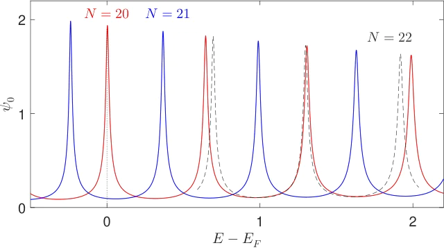
As expected, some states in the hybrid sample are resonant (\(E=E^{\,}_n\), where the index \(n\) corresponds to the number of electron half-wavelengths in the film) resembling both a particle in a box and standing waves in a parallel-plane resonator with low-transmission barriers. Figure 2 shows the dependence of the absolute value of the wave function at the film–vacuum interface, \(\psi^{\,}_0\), on the incident electron energy for two Pb(111) films of different thicknesses. When the thicknesses of two areas in the Pb(111) film differ by one monolayer (\(d^{\,}_{ML}=0.286\)nm according to standard crystallographic data for bulk crystals), the oscillations in the \(\psi^{\,}_0\) value as a function of \(E\) near the Fermi energy occur out of phase (compare the red--blue and blue--black pairs of curves). The appearance of a new resonant state with a pronounced tail in the barrier region should enhance the coupling with evanescent tip states (i.e., increase the overlap between \(\psi^{\,}_s\) and \(\psi^{\,}_t\)), thereby raising the tunneling current within a narrow energy window around \(E^{\,}_n\). When tunneling measurements are performed in the constant-current mode (with an active feedback loop), such oscillating coupling between \(\psi^{\,}_s\) and \(\psi^{\,}_t\) should be compensated by variations in the width of the tunneling barrier. This means that the difference between the apparent heights of flat terraces with different numbers of monolayers, as measured by scanning tunneling microscopy in the constant-current mode, should exhibit oscillatory and bias-dependent behavior. Such an effect was previously experimentally considered for Pb(111) films[25] in the range of bias voltage from 0.3 to 3 V. We now aim to reproduce this result for a new sample/tip and to extend this observation to thicker samples over a wider voltage range exceeding the work function.
Methods
Topography and local electronic properties of Pb(111) islands[4-6] grown on Si(111) wafers were investigated by means of low-temperature scanning tunneling microscopy (STM) and spectroscopy (STS). All measurements were carried out in an ultra-high vacuum (UHV) scanning probe microscopy system (Omicron Nanotechnology GmbH) operating at a base pressure of \(2\times 10^{-10}\)mbar. Thermal deposition of Pb (99.99% purity) from a Mo crucible was performed in situ onto the Si(111)\(7\times 7\) surface at room temperature using an electron-beam evaporator (Focus GmbH) at a pressure of \(6\times 10^{-10}\)mbar. All STM/STS measurements were carried out at liquid nitrogen temperature using electrochemically etched W tips cleaned by electron bombardment. To enhance topographic and spectral resolution, the tip apex was functionalized by picking up a small amount of lead through gentle contact with the surface in a peripheral region.
The surface topography was studied using a standard STM mode, i.e., by measuring the displacement of the tip mounted on a piezo-scanner while scanning over the sample surface with a constant sample bias voltage \(U\) (with respect to the virtually grounded tip) and tunneling current \(I\). Local electronic properties were studied by STS in constant-current mode with active feedback, where the tip–sample distance \(z\) varies as the bias voltage is changed.[25, 26]
Discussion
Figure 3 shows the topography image (panel a) and the map of the local variation of the tunneling conductance (panel b), both acquired simultaneously at \(U=0.40\) V. Dark and bright regions in the \(dI/dU\) map reveal the boundaries between areas of different local thicknesses. Two dashed lines in panel a mark the positions of two monatomic steps on the substrate. This indicates that the central part of the image (within the dotted rectangle) belongs to the same Si(111) terrace and contains no subsurface defects. Tunneling spectra for points 1 and 2 are presented in the inset of Figure 4b. Comparing the \(dI/dU\) maxima with the diagram in Ref. [9] identifies points 1 and 3 as a Pb terrace 31 monolayers thick, while point 2 corresponds to a thickness of 30 monolayers.
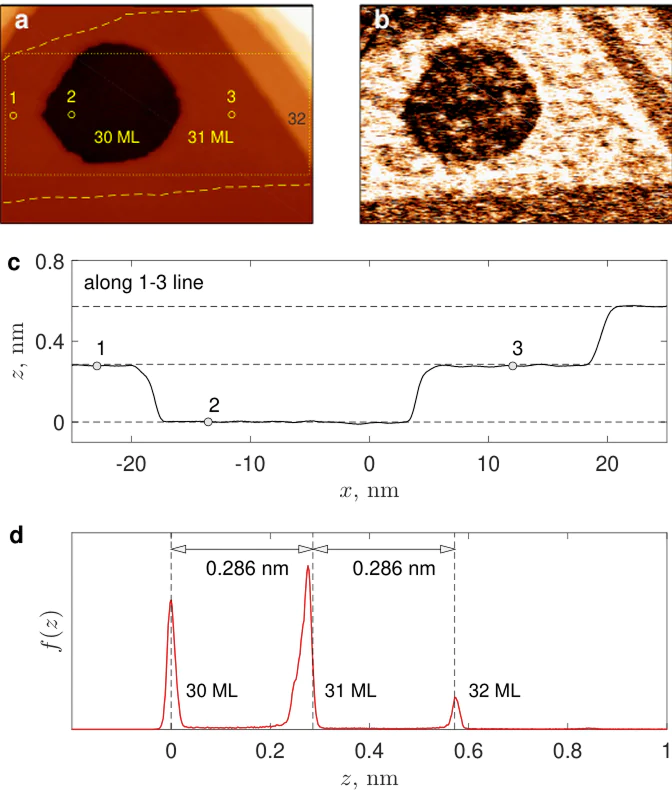
Figure 3c displays the cross-sectional profile of the topography image, while Figure 3d shows the probability density function \(f(z)\) of apparent heights, extracted from the area within the dotted rectangle in Figure 3a after plane subtraction and piezo-scanner calibration (see Ref. [25] for details). Three peaks in the \(f(z)\) distribution correspond to the Pb(111) terraces of different thicknesses: 30, 31 and 32 monolayers (from left to right). One can see that the apparent heights of the monatomic steps are not strictly constant. In particular, the step height between terraces of 30 and 31 monolayers is slightly smaller (about 5%) than the expected theoretical value \(d^{\,}_{ML}\), whereas the step height between terraces of 31 and 32 monolayers is slightly larger than \(d^{\,}_{ML}\). Notably, the step height between terraces of 30 and 32 monolayers is close to \(2d^{\,}_{ML}\) within experimental accuracy. The latter observation seems reasonable, if one takes into account that the spectrum of quantum-well states for the terraces of \(N\) and \(N+2\) monolayers should be rather close, provided \(N\gg 1\) and \(E\sim E^{\,}_F\) (see Figure 2).
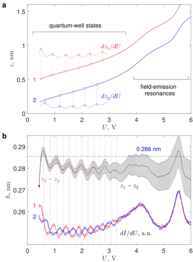
The dependences of the relative tip height \(z\) on \(U\) for points 1 and 2, acquired in constant-current mode, are shown in Figure 4a. These \(z-U\) curves are monotonically increasing functions, with periodic small-scale oscillations of the slope, typical of quantum-well states for \(|e|U\lesssim 3.5-4\) eV, and with pronounced aperiodic oscillations due to field-emission resonances at \(|e|U\gtrsim 4\) eV. It is evident that the bias-induced oscillations of \(dI/dU\) and \(dz/dU\) occur in phase: both \(dI/dU\) and \(dz/dU\) rapidly increase and then decrease as \(|e|U\) sweeps through one of the quantum-well states \(E^{\,}_n\), producing local maxima in both signals at \(|e|U\simeq E^{\,}_n\).
The difference \(h=z^{\,}_1-z^{\,}_2\), corresponding to the apparent height of the monatomic Pb(111) step in constant-current topographic mode, exhibits oscillatory behavior as a function of \(U\) (Figure 4b). We emphasize that the apparent heights reach their extremal values when the differential conductances of these two terraces become equal[25]. The bias voltages satisfying this condition are depicted by vertical dotted lines.
We can conclude that
(i) Such a small effect of the bias-induced oscillations of the visible height of the monatomic steps appears reproducible, since the main observations of this paper resemble the results of Ref. [25], obtained for a different sample/tip.
(ii) The period of these oscillations coincides with the period of the peaks in the \(dI/dU-U\) dependence, caused by resonant tunneling through the quantum-well states. The extrema of the monatomic step height are found to coincide with bias voltages where the differential tunneling conductances of terraces of different thicknesses are equal.
(iii) This effect can be regarded as instrumental: the geometric step height seems to be fixed, while the apparent height measured in constant-current STM contains bias-dependent and tip-dependent electronic contributions. Indeed, the modification of the shape of the STM tip after touching the sample surface affects the observed amplitude of the \(dI/dU\) and \(dz/dU\) oscillations for both quantum-well states and field-emission resonances. Consequently, the extent to which quantum-size effects manifest themselves in the oscillations of the visible tip height depends on the actual tip shape (about 5% for the present study and up to 10% for the data in Ref. [25]).
(iv) It is worth noting that pronounced changes in the apparent heights of monatomic steps on ultrathin Pb(111) films were reported by Su et al. [5] and explained in terms of structural relaxation of islands with even and odd numbers of monolayers (\(N=5, 6\) and 7). However, they did not study the effect as a function of bias voltage.
(v) According to Figure 4b, the oscillations in \(dI/dU\) become less pronounced with increasing bias voltage and become indistinguishable at high bias voltages exceeding the work function (\(\simeq 3.8\)eV). It is reasonable to assume that the bias dependence of the apparent step height should be suppressed at \(|e|U\gtrsim 4-5\)eV. However, reliable topographic data that would either confirm or refute this conclusion are not yet available.
(vi) According to Figure 2 and Figure 3d, the apparent height of the Pb(111) bilayer step for bias voltages around \(0.5-2\)V should be less sensitive to the voltage variations than the apparent height of the Pb(111) monatomic step.
Conclusion
Using low-temperature scanning tunneling microscopy and spectroscopy, we have investigated the bias dependence of the apparent height of Pb(111) steps formed by flat terraces of 30-32 monolayers thick. Our results show that the apparent height of a monatomic step on the Pb(111) surface, as measured by single-point \(z-U\) spectroscopy in constant-current mode, oscillates with bias voltage \(U\). We attribute this behaviour to the resonant tunneling through quantum-well states in thin Pb(111) films. The extrema in the apparent heights occur near crossings of the terrace-resolved differential conductances. We further find that the apparent height of the bilayer step is close to twice the bulk Pb(111) interplanar spacing within experimental uncertainty.
Acknowledgements
This study was supported by the Russian Science Foundation (project 23-72-30004).
Contact information
Corresponding author: Alexey Yu Aladyshkin,
orcid.org/0000-0001-5551-2474,
e-mail aladyshkin@ipmras.ru
*
Proceedings of the IV International Scientific School "Superconducting Functional Materials for Advanced Quantum Technologies 2026", September 21-25, 2026, Peterhof, Russia
Funders
References